Purpose
The RT4805A is a Boost converter with the input voltage range from 1.8V to 5V and provides 2A output current. This document explains the function and use of the RT4805A evaluation board (EVB), and provides information to enable operation, output voltage setting of the evaluation board.
Introduction
General Product Information
The RT4805A allows systems to take advantage of new battery chemistries that can supply significant energy when the battery voltage is lower than the required voltage for system power ICs. By combining built-in power transistors, synchronous rectification, and low supply current; this IC provides a compact solution for systems using advanced Li-Ion battery chemistries.
The RT4805A is a boost regulator designed to provide a minimum output voltage from a single-cell Li-Ion battery, even when the battery voltage is below system minimum. In boost mode, output voltage regulation is guaranteed to a maximum load current of 2A. Quiescent current in Shutdown Mode is less than 1µA, which maximizes battery life. The regulator transitions smoothly between Bypass and normal Boost Mode. The device can be forced into Bypass Mode to reduce quiescent current. The RT4805A is available in the WL-CSP-16B 1.67x1.67 (BSC) package.
Product Feature
-
4 Few External Components : 0.47μH Inductor and 0603 Case Size Input and Output Capacitors
-
Input Voltage Range : 1.8V to 5V
-
Output Range from 2.85V to 4.4V
-
VSEL = L 3.6V
-
VSEL = H 3.7V
-
Maximum Continuous Load Current : 2A at VIN > 2.65V Boosting VOUT to 3.35V
-
Up to 96% Efficient
-
True Bypass Operation when VIN > Target VOUT
-
Internal Synchronous Rectifier
-
True Load Disconnectwhen Shut Down
-
Forced Bypass Mode
-
VSEL Control to Optimize Target VOUT
-
Short-Circuit Protection
-
I2C Controlled Interface
-
Ultra low Operating Quiescent Current
-
Small WL-CSP 16B Package
Key Performance Summary
Table
|
Key Features
|
Evaluation Board Number : PCB089_V1
|
|
Default Input Voltage
|
3.0V
|
|
Max Output Current
|
2A
|
|
Default Output Voltage
|
Vout_H = 3.7V, Vout_L = 3.6V
|
|
Default Marking & Package Type
|
WL-CSP-16B 1.67x1.67 (BSC)
|
Bench Test Setup Conditions
Headers Description and Placement
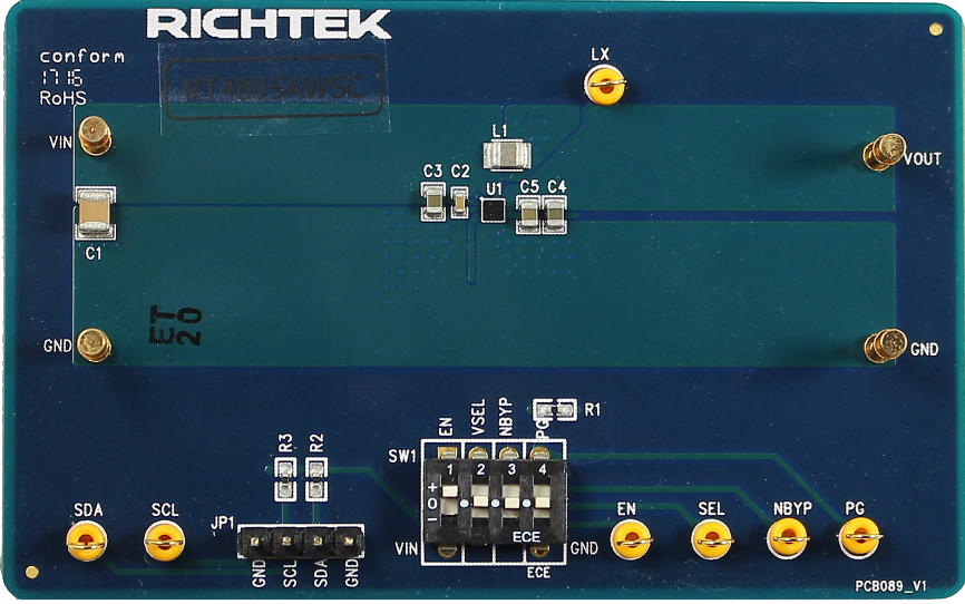
Carefully inspect all the components used in the EVB according to the following Bill of Materials table, and then make sure all the components are undamaged and correctly installed. If there is any missing or damaged component, which may occur during transportation, please contact our distributors or e-mail us at evb_service@richtek.com.
Test Points
The EVB is provided with the test points and pin names listed in the table below.
|
Test point/
Pin name
|
Signal
|
Comment (expected waveforms or voltage levels on test points)
|
|
VIN
|
Input voltage
|
Input voltage with range 1.8V to 5V.
|
|
EN
|
VOUT Enable
|
Enable control pin for VOUT.
|
|
LX
|
Switching Node
|
Switching Node.
|
|
PGND/AGND
|
Ground
|
Ground.
|
|
SDA/SCL
|
I2C Control
|
Pins to set functions such as VOUT, ILIM.
|
|
VOUT
|
Output Voltage
|
Default voltage : 5V ± 2%.
|
|
PGOOD
|
Power Good
|
Power Good. It is a open-drain output. PGOOD pin pulls low automatically if the overload or OTP event occurs.
|
|
VSEL
|
VOUT Select GPIO
|
Output Voltage Select. When boost is running, this pin can be used to select output voltage.
|
|
nBYP
|
Inverse Bypass Signal
|
Bypass. This pin can be used to activate Forced Bypass Mode. When this pin is LOW, the bypass switches are turned on and the IC is otherwise inactive.
|
Power-up & Measurement Procedure
1. Connect input voltage (1.8V < VIN < 5.0V).
2. To use a switch at “H” option to tie EN pin to input voltage VIN via SW1 or external voltage for enabling the device. Inversely, to use a jumper at “L” option to tie EN pin to ground GND for disabling the device.
3. To verify the output voltage VOUT via the I2C interface.
4. To connect an external load up to 1A and verify the output voltage and current.
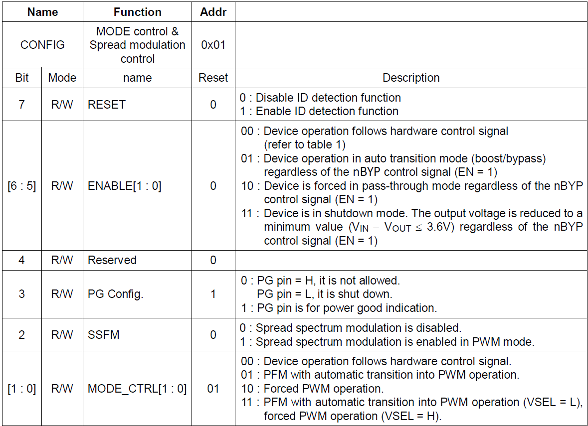
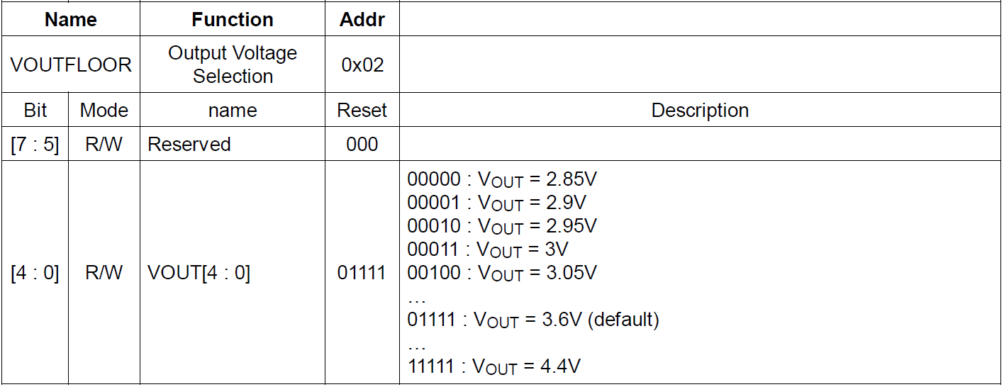
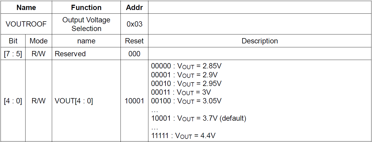
I2C Register Setting
The register as the table shown can be programmed by a MCU through the dedicated I2C interface. The device slave address is 0x39.
Schematic, Bill of Materials & Board Layout
EVB Schematic Diagram
Bill of Materials
|
Reference
|
Qty
|
Part number
|
Description
|
Package
|
Manufacture
|
|
U1
|
1
|
RT4805AWSC
|
Boost Converter
|
WL-CSP-16B 1.67x1.67
|
Richtek
|
|
C1
|
1
|
GRM32ER61A107ME20L
|
100μF/10V/X5R/1210
|
C-1210
|
Murata
|
|
C2
|
1
|
GRM188R61H105KAAL
|
1.0μF/50V/X7R/0603
|
C-0603
|
Murata
|
|
C3
|
1
|
EMK212ABJ106KG
|
10μF/16V/X7R/0805
|
C-0805
|
Taiyo
|
|
C4, C5
|
2
|
LMK212BBJ226MG
|
22μF/6.3V/X7R/0805
|
C-0805
|
Taiyo
|
|
L1
|
1
|
DFE2520F-R47M
|
0.47μH
|
L-2520
|
TOKO
|
|
R1
|
1
|
PFR05105FNH
|
1MΩ/0402/1%
|
R-0402
|
乾坤
|
|
R2, R3
|
2
|
PFR05102FNH
|
1kΩ/0402/1%
|
R-0402
|
乾坤
|
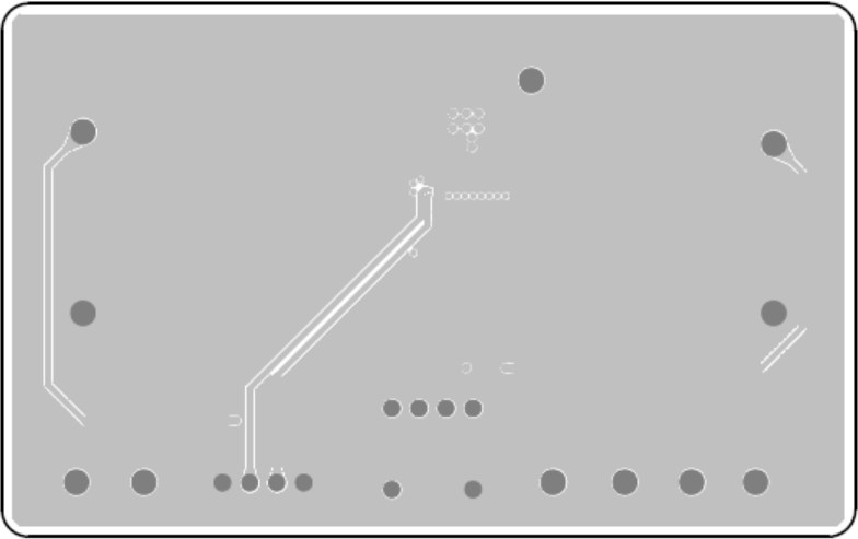
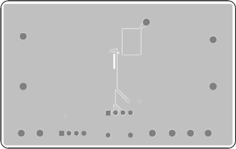
PCB Layout
Top View (1st layer)

PCB Layout—Inner Side (2nd Layer)
PCB Layout—Inner Side (3rd Layer)
Bottom View (4th Layer)